Samsung reckon that geopolitical uncertainties were likely to dampen demand for semiconductors until early 2023.Source: Samsung
Semiconductor superpower: Samsung beats TSMC with the the world’s first 3nm chips
- Samsung took on TSMC by initiating the mass production of the world’s first 3nm chips — that too using the Gate-All-Around (GAA) transistor architecture.
- The first batch of the semiconductor chips are made for high performance, low power computing applications and Samsung plans to expand to mobile processors next.
- The 3nm process brings 45% more reduced power usage, 23% improved performance and 16% smaller surface area compared to the 5nm process.
Two months ago, we wrote about the possibility of South Korean tech giant Samsung Electronics Co surpassing the world’s largest contract manufacturer of semiconductor chips, Taiwan Semiconductor Manufacturing Co (TMSC), when it comes to releasing the most advanced chips in the world. TSMC, despite having begun the pilot production of 3nm chips a while ago, may have just lost the race to Samsung.
The South Korean conglomerate has now announced that it has started the initial production of its 3-nanometer (nm) process node, automatically making it the leader when it comes to conquering the most advanced process technology at this point. In short, TSMC, the largest most significant supplier to Apple, has a lot of catching up to do.
In an announcement, Samsung said it is applying its Gate-All-Around (GAA) transistor architecture for the first time ever, on a surface that has a 16% smaller surface area than before. The new fabrication process is also 45% more power efficient while delivering 23% better performance than the previous 5nm process.

Samsung’s semiconductor manufacturing plant in Hwaseong, South Korea. Source: Samsung
With that, it defies the performance limitations of FinFET, improving power efficiency by reducing the supply voltage level, while also enhancing performance by increasing drive current capability. Samsung also said the process would be used for “high performance, low power computing” with mobile processors coming later.
Later on, the second-generation 3nm process will reduce power consumption by 50% and improve performance by 30% on a 35% reduced area. Samsung Electronics’ president and head of foundry business Siyoung Choi also highlighted the company’s goal to continue seeking “this leadership with the world’s first 3nm process with the MBCFET™. We will continue active innovation in competitive technology development and build processes that help expedite the achieving maturity of technology.”
It is however fair to note that despite overtaking TSMC with the world’s first 3nm, the Korean tech giant has a long road ahead to prove itself against the Taiwanese chipmaker that dominates market share and manufactures the chips for Apple’s iPhones, iPads, MacBooks, and Macs, plus supplies wafers to fabless semiconductor companies like Nvidia and AMD. For context, TSMC currently accounts for more than half of the global foundry business by revenue, Bloomberg reports.
3nm mass production from the Taiwanese chipmaker will apparently commence in the second half of the year, TSMC has said. Meanwhile, Samsung will go on producing 3nm chips at its Hwaseong facilities and is expected to extend that production to its newest Pyeongtaek fab.
The 3nm design technology by Samsung
Most interestingly, Samsung’s proprietary technology utilizes nanosheets with wider channels, which allow higher performance and greater energy efficiency compared to GAA technologies using nanowires with narrower channels. To put it simply, by utilizing the 3nm GAA technology, Samsung will be able to adjust the channel width of the nanosheet in order to optimize power usage and performance to meet various customer needs.

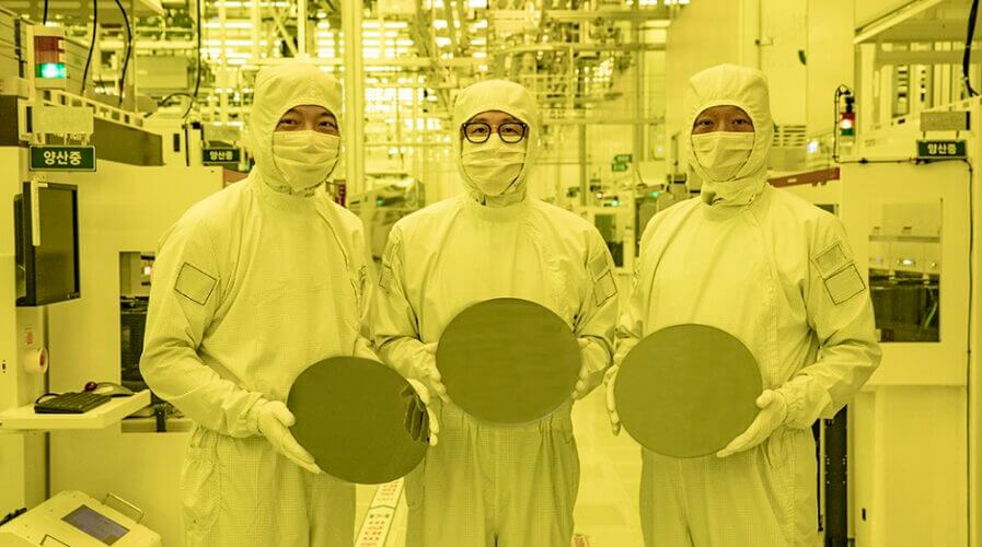
The leaders of Samsung Foundry Business and Semiconductor R&D Center are holding up three fingers as a symbol of 3nm celebrating the company’s first ever production of 3nm process with GAA architecture. Source: Samsung
Additionally, as technology nodes get smaller and chip performance needs grow greater, IC designers face challenges of handling tremendous amounts of data to verify complex products with more functions and tighter scaling. “To meet such demands, Samsung strives to provide a more stable design environment to help reduce the time required for design, verification and sign-off process, while also boosting product reliability,” it said.
In fact, since the third quarter of 2021, Samsung Electronics has been providing proven design infrastructure through extensive preparation with Samsung Advanced Foundry Ecosystem (SAFE) partners including Ansys, Cadence, Siemens and Synopsys, to help customers perfect their product in a reduced period of time.
TSMC’s market share still remains unfazed
Bloomberg Intelligence analyst Charles Shum reckons that Samsung’s launch of 3nm node chip production, based on a new-generation transistor architecture, shouldn’t affect TSMC’s market share and sales growth in the next 12 months. “Despite stronger performance, Samsung’s 3nm chip needs to demonstrate it can be produced at the same cost-efficiency level as TSMC’s most advanced N3 process before it can gain new orders from Apple, Qualcomm and other large chip designers,” he said.
Despite the fact that the Samsung foundries are only in their sixth year as a fully separate business unit, they are not far behind TSMC in terms of clients served. Although experts may still consider Samsung’s yields to be lower than those of its Taiwanese rival, the South Korean conglomerate is constantly investing and improving its manufacturing lines, with a clear goal of overtaking TSMC by 2030.
Undoubtedly, TSMC has also been competing fiercely with Samsung Electronics for 5nm and less, with Intel also competing in this battle. Data by TrendForce shows that TSMC is ranked with 52.1% of the market share established (based on sales) in the fourth quarter of last year, followed by Samsung Electronics with 18.3% and second place.
READ MORE
- Data Strategies That Dictate Legacy Overhaul Methods for Established Banks
- Securing Data: A Guide to Navigating Australian Privacy Regulations
- Ethical Threads: Transforming Fashion with Trust and Transparency
- Top 5 Drivers Shaping IT Budgets This Financial Year
- Beyond Connectivity: How Wireless Site Surveys Enhance Tomorrow’s Business Network


